Update: This entry took 2nd place in the 7400 Competition. I won a Parallax Boe-Bot Robot Kit. Thanks Parallax! Thanks Ian!
Don’t listen to goatee Spock. He’s evil! This entry for Dangerous Prototypes’ Open 7400 Logic Competition is most illogical and at least somewhat fascinating. In this article I’ll demonstrate how you can use the internal protection diodes and back powering to power a 74HC14 at a voltage “double” (minus diode drops) that of the primary power supply. I call this circuit an illogical doubler mostly as a pun because the 74HC14 is a logic chip but also because of the quirky way it works. Perhaps “ill-understood” (by me) is a more apt description for the latter case.
Introductory Concepts
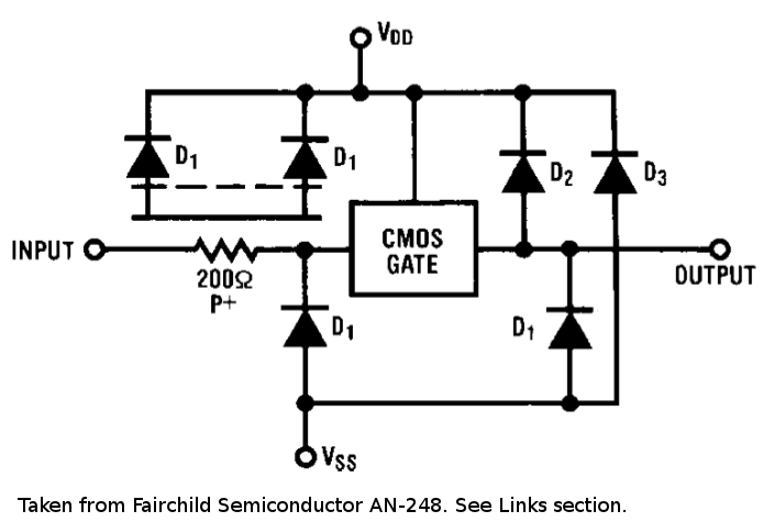
Most HCMOS devices have input and output protection circuitry to prevent ESD damage to the MOSFETs which make up the integrated circuit. How the protection circuitry is implemented varies among the devices and semiconductor manufacturers, but the usual way is to use clamping diodes to keep over/undervoltages away from the MOSFETs’ sensitive gates. The protection diode from an I/O pin to VDD can be a bother to hardware tinkerers because it will conduct if the IC’s power pin is disconnected and the I/O pin has a voltage on it resulting in the IC being powered by the I/O pin. This is known as back powering.
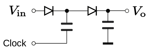
The Dickson doubler is a clever little circuit. It’s a type of charge pump voltage multiplier. When Clock goes low the input capacitor is charged via Vin and when Clock goes high it pushes the charge on the input capacitor onto the output cap. The diodes are necessary to make the charge flow in the desired direction. The output voltage of the Dickson doubler is only twice the input when the voltage drop caused by the diodes is negligible compared to 2*Vin.
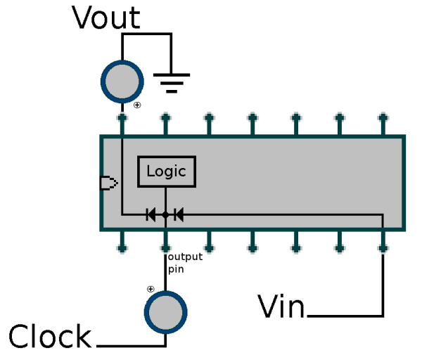
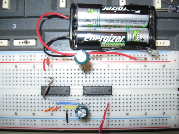
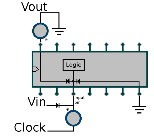
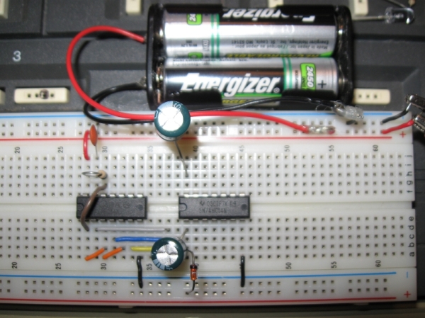
Notice that the protected pins on a HCMOS IC have incoming and outgoing diodes just like the first capacitor in a Dickson doubler. Therefore if we connect Vin to the ground pin (i.e. VSS), the positive leg of a capacitor to a diode protected I/O pin and the negative leg to a clock source, then connect the positive leg of a second capacitor to the IC’s power pin (i.e. VDD) and the negative leg to ground, we’ll should be able to use the protection diodes to back power the IC at double the voltage Vin minus the voltage drop caused by the diodes. That’s the idea at least, but there are a few quirks that I’ll explain as we go along. To test the illogical Dickson doubler I used two SN74HC14N ICs. The one on the left generated the clock source and the right one served as the victim back powered doubler.
Output Pin Illogical Doubler
Oddly, the illogical doubler only works when the input capacitor is connected to an output pin. Even stranger, the doubler still works, better in fact, if Vin is connected to another output pin instead of ground; in this case, I don’t know what path the charging current takes to get from Vin to the input capacitor.
This video demonstrates using the protection diodes of a 74HC14 as part of a Dickson doubler. The UV LED (3.6V @ 20 mA) is only dimly lit by the voltage supplied by the batteries. The doubler increases the voltage from 2.68 V to 4.35 V which is 1.01 volts less than twice the input voltage. Although it is difficult to see in this video, when the LED is connected to the higher voltage it outputs more light. Next the input voltage wire is moved from ground to an output pin to show that the doubler still functions when an output is used. Finally the effects of lowering the clock frequency are shown by inserting a 0.1 uF capacitor in the clock circuitry.
Input Pin Illogical Doubler
Unfortunately the “output pin illogical doubler” doesn’t function properly when the ground pin is grounded even if Vin is fed into an output pin instead of the ground pin. Without a ground all the circuit can do is provide a higher voltage. However, by moving the input capacitor to an input pin and providing Vin through a separate diode connected to the same pin we’re able to sneak power through the protection diode, get a higher voltage, and use the 74HC14 normally.
In this video the illogical doubler increases the voltage from 2.68 V to 3.90 V which is 1.46 volts less than twice the input voltage. When the LED is connected to the higher voltage it outputs more light compared to when it was powered by the batteries alone. Next a 10 Megohm resistor is connected from the output pin to the input pin which forms an RC circuit with the 0.1 uF cap that is connected to the input pin and ground. The RC circuit causes the output to oscillate thereby demonstrating that the 74HC14 still functions normally.
Final Thoughts
Because the illogical doubler only uses the internal protection diodes it should work with ICs other than the 74HC14. I was able to get 4.6 V from 2.68 V using an SN74HC595N configured as an output illogical doubler. I didn’t blow a single pin while playing with any of my chips. They didn’t even get hot, but TI’s datasheets say the input/output clamp current is only ±20 mA, so don’t overload them. You may be wondering if it is possible for the back powered 74HC14 to provide it’s own Clock signal; I tried it and it doesn’t work. When Clock is pulling the input capacitor charges as expected; however, when Clock goes high a path is created for the input capacitor to discharge itself that doesn’t go through the output capacitor. For best results with a charge pump, you should optimize the frequency and capacitor values. I didn’t see the point in doing this because I thought it insane to use one of these circuits for anything but a laugh. For the frequency, I ran the 74HC14 Clock as fast as it would go. In general a faster frequency worked better, but I’ve read that there is a point where you lose more from parasitic capacitive losses than you gain by going faster. For the capacitor values I simply used two 100 uF, 50 V electrolytics. I’m not an expert in charge pumps. I simply used trial and error to find values that worked. If you can shed light on how the output pin illogical doubler with Vin supplied through an output pin instead of ground works, have a correction, or anything at all to share, then please leave a comment!
Electrostatic Discharge: Understand, Simulate, and Fix ESD Problems. Appendix A

[…] [Jonathan Thomson] just finished writing up his entry for the 7400 logic contest. It’s a voltage doubler that uses a 74HC14 logic chip. Because this is not at all what the chip was meant for–and he’s a sucker for puns–he’s calling it the Illogical Dickson Doubler. […]
What capacitor values did you use?
I used 100 uF 50 V electrolytics. I didn’t try to optimize the capacitor values I used.
Here’s a useful link that one of the other 7400 competition entries provided for his article.
Click to access 607PET22a.pdf
[…] In this article it has been shown how one can use the internal protection diodes and the back powering to power up a 74HC14 at double voltage to the voltage of the primary power supply. This circuit mechanism is called as the Illogical Dickson Doubler. […]